Old Phone to USB Drive: How to Turn a Dead Phone's Chip Into a Fast Flash Drive | yunpoly
Everyone has a drawer of retired phones: cracked screens, swollen batteries, boot loops that take forever. Most of them end up sold for pocket change, traded for a stainless steel basin, or left to gather dust. But inside that "e-waste" hides a genuinely capable component — the eMMC or UFS storage chip on the mainboard, which is essentially a high-performance flash memory. With a little soldering, that chip becomes a custom USB drive that reads faster than most store-bought sticks.
The whole project costs about 30 yuan (~$5) in parts. Here is how it works, step by step.
Step 1: Remove the "Retired" Chip
Start by heating the phone's back cover — a hairdryer on hot, circled over the panel for about a minute — then work the seam open with a suction cup and a plastic spudger.
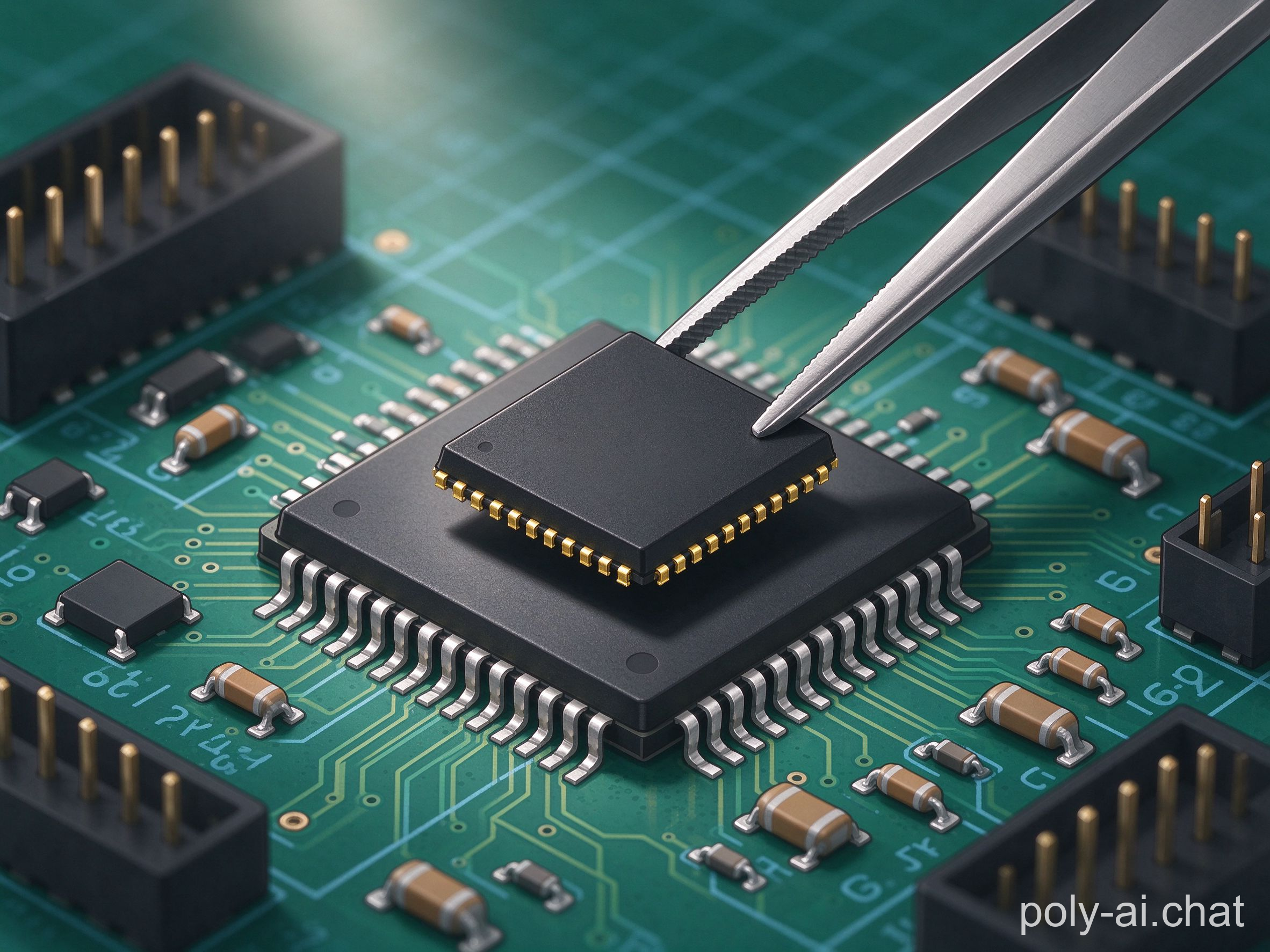
The first rule is safety: disconnect the battery ribbon cable before touching anything else. Then find the black square chip on the mainboard stamped with a "Samsung", "Toshiba", or "SanDisk" logo — that is the eMMC or UFS storage. It sits surrounded by a crowd of tiny resistors.
Use a hot-air rework station set to around 350°C at moderate airflow, sweep the nozzle around the chip's edges for about 40 seconds until the solder melts, and lift it free with tweezers.
No hot-air station? There is a "soft mod" alternative: buy a matching no-solder USB controller board, read the chip's info through a data cable, and mount the whole mainboard inside an acrylic enclosure. It works, but it skips the fun.
Step 2: Give the Chip a New Home — Solder It to a Controller Board
Order a matching USB flash controller board — common options are the NS1081 or SM3350, and the chip protocol must match. You will also need a fine-tipped soldering iron, flux, and 0.3 mm solder wire.
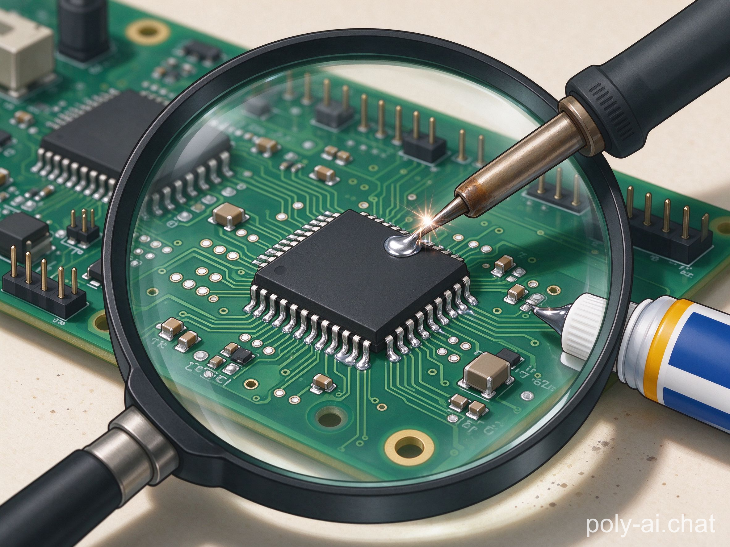
Apply a thin coat of flux to the chip's pads, align it with the board's pad markings (usually a small dot marks pin 1), and drag-solder around all four sides. The molten solder will distribute evenly under surface tension. If neighboring pins bridge, a bit of solder wick cleans them up.
This step tests patience — but when the four sides gleam silver under a magnifier, the payoff is real.
Step 3: Plug In and Rebuild the Drive's Identity
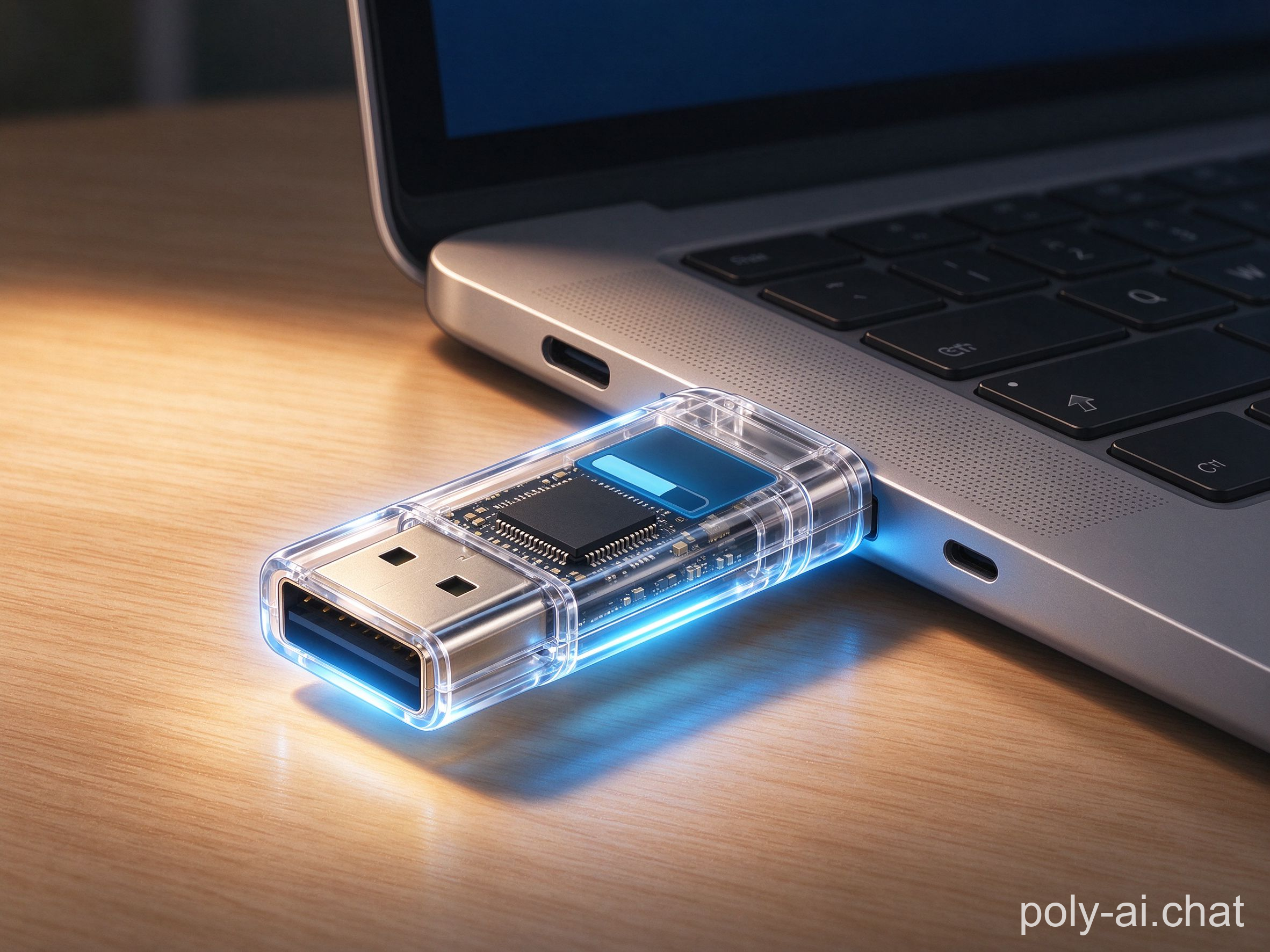
Insert the controller board into a USB port and the system will detect new hardware. Open the mass-production tool (usually provided by the board seller), let it identify the chip capacity, set the drive name, and hit Start. When the progress bar finishes, a dead phone chip officially has a new life as a USB drive.
Performance is the pleasant surprise: a typical eMMC 5.1 chip reads around 150 MB/s and writes about 40 MB/s — roughly three times faster than an ordinary USB 2.0 stick. Large file transfers stop being a chore.
Step 4: Armor the Bare Board
A naked controller board risks shorting out. The simplest wrap is heat-shrink tubing; for looks, try a transparent resin USB shell, a 3D-printed case, or even an old lighter or lipstick tube. Engrave the model of the donor phone on the shell — "iPhone 6s, reincarnated" — and the drive carries a story.
Why Bother?
This is not about saving money — the materials cost about 30 yuan. It is a small act of resistance against planned obsolescence. That phone once held your photos, playlists, and chat history. Now it sheds its "smart" burden and keeps serving you in the most humble storage form. The capacity number your computer shows is not just flash memory; it is the warmth of something that used to sit in your hand.
Two warnings, repeated: never puncture the battery while removing it; solder in a ventilated room; and do not check "erase all blocks" in the mass-production tool — that wipes the chip's data for good. If you melt a chip on your first attempt, that failed chip still makes a unique keychain.

References:
[1] All illustrations are AI-generated.
[2] Locally adapted from a public DIY guide on salvaging phone storage chips into USB drives, 2026-09-26.
- Bill Gates Warns AI Could Kill a Billion People — and Says Self-Regulation Has Failed
- The "Textbook Diet": 7 Nutrition Rules Most Diet Advice Misses
- Flu Season Is Back: Why the Annual Flu Shot Is a Biology Lesson Worth Taking
- Matcha Benefits: What 3 Grams of Matcha Powder Actually Contains
- The 60-cm Long Egg Tart Is Delicious for 3 Bites — Then Sickeningly Rich. Here's the Biology
- Pepino Melon Is Sweet, Low-Calorie, and 94% Water — If You Buy It Ripe
- Old Phone to USB Drive: How to Turn a Dead Phone's Chip Into a Fast Flash Drive | yunpoly
- Trump Wants to Rename AI to "SI" — Because "Artificial" Makes Intelligence Sound Fake
- A 1 cm Thyroid Nodule Turned Out to Be Cancer While a Bigger One Was Fine — Here's the Biology
- Why Are Mysterious Round Holes Appearing on Parked Cars? The Culprit Is a Moth Larva
全部评论